Inference and PCM statistical model
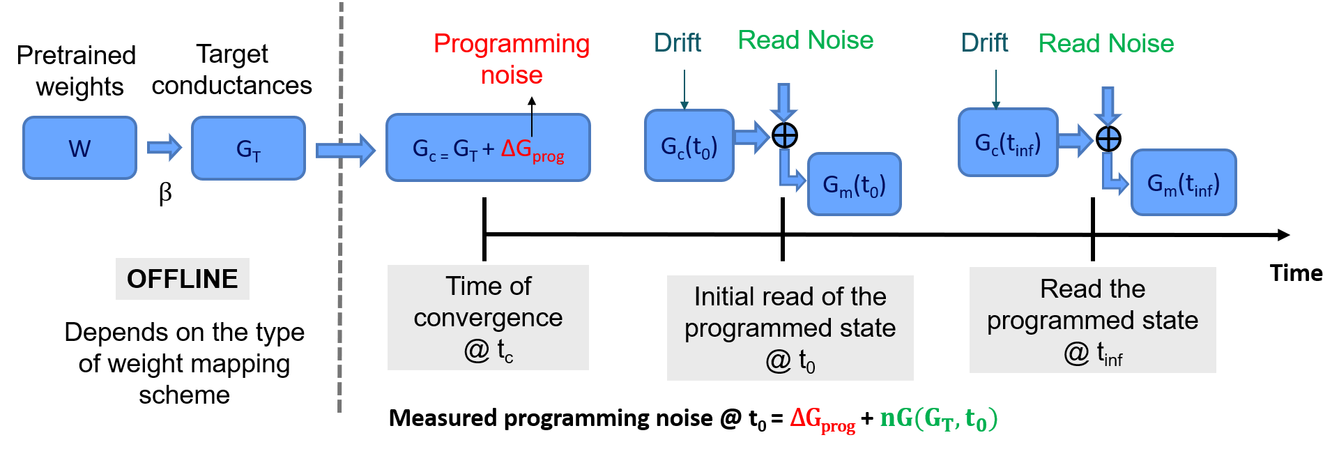
The analog AI hardware kit provides a state-of-the-art statistical model of a phase-change memory (PCM) array that can be used when performing inference to simulate the various sources of noise that are present in a real hardware [1]. This model is calibrated based on extensive measurements performed on an array containing 1 million PCM devices fabricated at IBM [2].
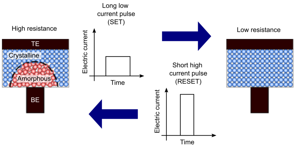
PCM is a key enabling technology for non-volatile electrical data storage at the nanometer scale, which can be used for analog AI [3]. A PCM device consists of a small active volume of phase-change material sandwiched between two electrodes. In PCM, data is stored by using the electrical resistance contrast between a high-conductive crystalline phase and a low-conductive amorphous phase of the phase-change material. The phase-change material can be switched from low to high conductive state, and vice-versa, through applying electrical current pulses. The stored data can be retrieved by measuring the electrical resistance of the PCM device. An appealing attribute of PCM is that the stored data is retained for a very long time (typically 10 years at room temperature), but is written in only a few nanoseconds.
The model simulates three different sources of noise from the PCM array: programming noise, read noise and temporal drift. The model is only used during inference and therefore it is assumed that network weights have been trained beforehand in software. The diagram below explains how these three sources of noise are incorporated during inference when using the statistical model:
Mapping the trained weights to target conductances
This step is typically done offline, after training, before programming the hardware. When the final converged network weights \(W\) have been obtained after training, they must be converted to target conductance values \(G_T\) that will be programmed on the hardware, within the range that it supports. In the statistical model, this range is set to \([0,1]\), where \(1\) corresponds to the largest conductance value \(g_\text{max}\) that can be reliably programmed on the hardware.
The statistical model assumes that each weight is programmed on two PCM devices in a differential configuration. That is, depending on the sign of the weight, either the device encoding the positive part of the weight or the negative part is programmed, and the other device is set to 0. Thus, the simplest way to map the weights to conductances is to multiply the weights by scaling factor \(\beta\), which is different for every network layer. A simple approach is to use \(\beta = 1/w_\text{max}\), where \(w_\text{max}\) is the maximum absolute weight value of a layer.
Programming noise
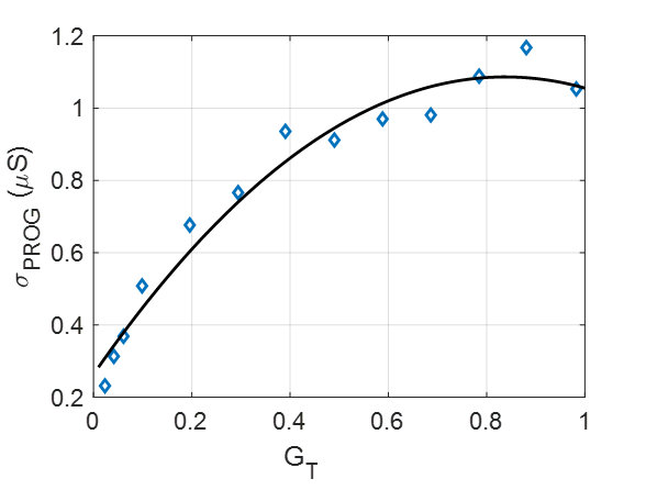
After the target conductances have been defined, they are programmed on the PCM devices of the hardware using a closed-loop iterative write-read-verify scheme [4]. The conductance values programmed in this way on the hardware will have a certain error compared with the target values. This error is characterized by the programming noise. The programming noise is modeled based on the standard deviation of the iteratively programmed conductance values measured from hardware.
The equations used in the statistical model to implement the programming noise are (where we use small letters for the elements of the matrices \(W\) and \(G_T\), etc., and omit the indeces for brevity):
The fit between this equation and the hardware measurement is shown below:
Drift
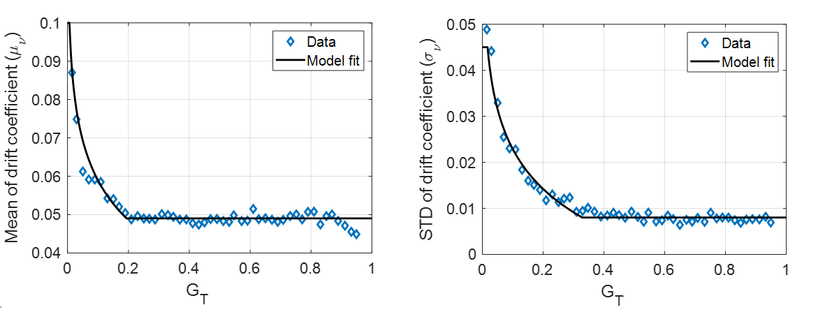
After they have been programmed, the conductance values of PCM devices drift over time. This drift is an intrinsic property of the phase-change material of a PCM device and is due to structural relaxation of the amorphous phase [5]. Knowing the conductance at time \(t_c\) from the last programming pulse, \(g_\text{prog}\), the conductance evolution can be modeled as:
where \(\nu\) is the so-called drift exponent and is sampled from \({\cal N}(\mu_\nu,\sigma_\nu)\). \(\nu\) exhibits variability across a PCM array and a dependence on the target conductance state \(g_T\). The mean drift exponent \(\mu_\nu\) and its standard deviation \(\sigma_\nu\) measured from hardware can be modeled with the following equations:
The fits between these equations and the hardware measurements are shown below:
Read noise
When performing a matrix-vector multiplication with the in-memory computing hardware, after the weights have been programmed, there will be instantaneous fluctuations on the hardware conductances due to the intrinsic noise from the PCM devices. PCM exhibits \(1/f\) noise and random telegraph noise characteristics, which alter the effective conductance values used for computation. This noise is referred to as read noise, because it occurs when the devices are read after they have been programmed.
The power spectral density \(S_G\) of the \(1/f\) noise in PCM is given by the following relationship:
The standard deviation of the read noise \(\sigma_{nG}\) at time \(t\) is obtained by integrating the above equation over the measurement bandwidth:
where \(t_{read} = 250\) ns is the width of the pulse applied when reading the devices.
The \(Q_s\) measured from the PCM devices as a function of \(g_T\) is given by:
The final simulated PCM conductance from the model at time \(t\), \(g(t)\), is given by:
Compensation method to mitigate the effect of drift
The conductance drift of PCM devices can have a very detrimental effect on the inference performance of a model mapped to hardware. This is because the magnitude of the PCM weights gradually reduces over time due to drift and this prevents the activations from properly propagating throughout the network. A simple global scaling calibration procedure can be used to compensate for the effect of drift on the matrix-vector multiplications performed with PCM crossbars. As proposed in [5], the summed current of a subset of the columns in the array can be periodically read over time at a constant voltage. The resulting total current is then divided by the summed current of the same columns but read at time \(t_0\). This results in a single scaling factor, \(\hat{\alpha}\), that can be applied to the output of the entire crossbar in order to compensate for a global conductance shift.
The figure below explains how the drift calibration procedure can be performed in hardware:
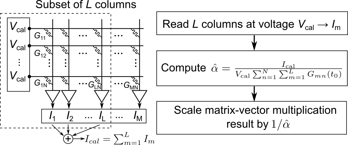
In the simulator, we implement drift compensation by performing a forward pass with an all 1-vector as an input, and then summing outputs (using the potential non-idealities defined for the forward pass) in an absolute way. This procedure is done once after programming and once after applying the drift expected as time point of inference \(t_\text{inference}\). The ratio of the two numbers is the global drift compensation scaling factor of that layer, and it is applied (in digital) to the (digital) output of the analog tile.
Note that the drift compensation class
BaseDriftCompensation is user
extendable, so that new drift compensation methods can be added
easily.
Example of how to use the PCM noise model for inference
The above noise model for inference can be used in our package
in the following way. Instead of using a regular analog tile, that is catered
to doing training on analog with pulsed update and others (see Section
Using analog tiles), you can use an _inference_ tile that
only has non-idealities in the forward pass, but a perfect update and
backward pass. Moreover, for inference, weights can be subject to
realistic weight noise and drift as described above. To enable this
inference features, one has to build an model using our
InferenceTile (see also
example 5):
# Define a single-layer network, using inference/hardware-aware training tile
rpu_config = InferenceRPUConfig()

# specify additional options of the non-idealities in forward to your liking
rpu_config.forward.inp_res = 1/64.  # 6-bit DAC discretization.
rpu_config.forward.out_res = 1/256. # 8-bit ADC discretization.
rpu_config.forward.w_noise_type = OutputWeightNoiseType.ADDITIVE_CONSTANT
rpu_config.forward.w_noise = 0.02   # Some short-term w-noise.
rpu_config.forward.out_noise = 0.02 # Some output noise.

# specify the noise model to be used for inference only
rpu_config.noise_model = PCMLikeNoiseModel(g_max=25.0) # the model described

# specify the drift compensation
rpu_config.drift_compensation = GlobalDriftCompensation()

# build the model (here just one simple linear layer)
model = AnalogLinear(4, 2, rpu_config=rpu_config)
Once the DNN is trained (automatically using hardware-aware training, if the forward pass has some non-idealities and noise included), then the inference with drift and drift compensation is done in the following manner:
model.eval()        # model needs to be in inference mode
t_inference = 3600. # time of inference in seconds (after programming)

program_analog_weights(model) # can also omitted as it is called below in any case
drift_analog_weights(model, t_inference) # modifies weights according to noise model

# now the model can be evaluated with programmed/drifted/compensated weights
Note that we here have two types of non-linearities included. For the first, longer-term weight noise and drift (as described above), we assume that during the evaluation the weight related PCM noise and the drift is done once and then weights are kept constant. Thus, a subsequent test error calculation over the full test set would signify the expected test error for the model at a given time. Ideally, one would want to repeat this for different weight noise and drift instance and or different inference times to access the accuracy degradation properly.
The second type of non-idealities are short-term and on the level of
a single analog MACC (Multiply and Accumulate). Noise on that level vary
with each usage of the analog tile and are specified in the
rpu_config.forward.
For details on the implementation of our inference noise model, please
consult PCMLikeNoiseModel. In
particular, we use a
SinglePairConductanceConverter
to convert weights into conductance paris and then apply the noise pn
both of these pairs. More elaborate mapping schemes can be
incorporated by extending
BaseConductanceConverter.
References
[1] Nandakumar, S. R., Boybat, I., Joshi, V., Piveteau, C., Le Gallo, M., Rajendran, B., … & Eleftheriou, E. Phase-change memory models for deep learning training and inference. In 26th IEEE International Conference on Electronics, Circuits and Systems (ICECS) (pp. 727-730). 2019
[2] Joshi, V., Le Gallo, M., Haefeli, S., Boybat, I., Nandakumar, S. R., Piveteau, C., … & Eleftheriou, E. Accurate deep neural network inference using computational phase-change memory. Nature Communications, 11, 2473. 2020
[3] Le Gallo, M., & Sebastian, A. An overview of phase-change memory device physics. Journal of Physics D: Applied Physics, 53(21), 213002. 2020
[4] Papandreou, N., Pozidis, H., Pantazi, A., Sebastian, A., Breitwisch, M., Lam, C., & Eleftheriou, E. Programming algorithms for multilevel phase-change memory. In IEEE International Symposium of Circuits and Systems (ISCAS) (pp. 329-332). 2011
[5] Le Gallo, M., Krebs, D., Zipoli, F., Salinga, M., & Sebastian, A. Collective Structural Relaxation in Phase‐Change Memory Devices. Advanced Electronic Materials, 4(9), 1700627. 2018
[6] Le Gallo, M., Sebastian, A., Cherubini, G., Giefers, H., & Eleftheriou, E. Compressed sensing with approximate message passing using in-memory computing. IEEE Transactions on Electron Devices, 65(10), 4304-4312. 2018